Samsung's latest Exynos 2400 chipset, powering the Galaxy S24 and Galaxy S24+ smartphones, brings a notable advancement to the table with the implementation of Fan-Out Wafer Level Packaging (FOWLP) technology. With the upgraded chip packaging tech, the Exynos 2400 reportedly delivers better performance and thermals.
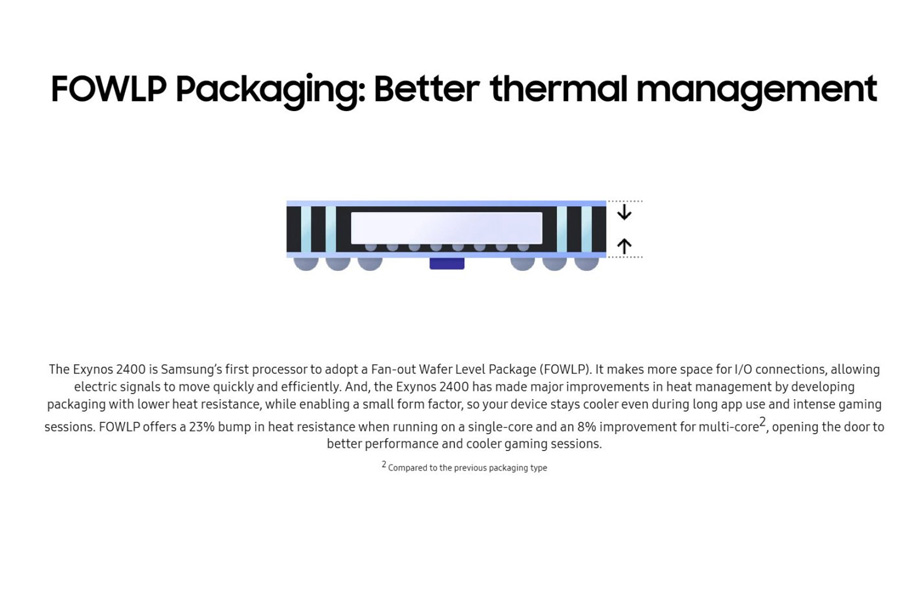 Compared to the conventional FCBGA (Flip Chip Ball Grid Array) chip packaging tech, FOWLP delivers lower thermal resistance and a slimmer package. The Exynos 2400 marks Samsung's first chip to utilize FOWLP, and the company claims a 23% and 8% increase in heat resistance in single-core and multi-core performance, respectively.
What is FOWLP?
Fan-out Wafer Level Packaging (FOWLP) enhances semiconductor integration, using cost-effective materials like epoxy mold compound (EMC) to embed dies and increase I/O connections without requiring expensive silicon space.- Also, read
- Samsung announces the pre-booking of Galaxy S24 Ultra in Nepal
- Samsung Galaxy S24 and S24 Plus launched in Nepal with tons of AI!
- Asus ROG Zephyrus G16 (2024) to come with Intel Core Ultra processors!
Exynos 2400 performance benchmarks
According to a report by an X (formerly Twitter) userNo gallery images available
While the Exynos 2400 impressed in both of those GPU benchmarking tools, Samsung's latest chip fell behind the Snapdragon 8 Gen 3 in AnTuTu. According to a test performed by YouTuber "Khôi Ngọng", the Snapdragon 8 Gen 3 on the S24 Ultra posted a little over 1.8 million while the Exynos 2400 maxed out at 1.7 million points only.
Exynos 2400 Overview:
CPU and GPU
As for the chip itself, it is manufactured under Samsung's 4nm LPP+ node. The Exynos 2400 brags a deca-core CPU setup, which includes a high-performance Cortex-X4 (@3.2 GHz), along with two Cortex-A720 (@2.9 GHz), three Cortex-A720 (@2.6 GHz), and four Cortex-A520 (@2.0 GHz) cores. Whereas the Exynos 2400 is equipped with the Samsung Xclipse 940 GPU built on AMD's RDNA 3 architecture. It supports all the flagship features too. Like hardware-based ray tracing, variable rate shading, and an upscaling tech called "FidelityFX Super Resolution".Memory and NPU
Other than this, Samsung's latest flagship chip supports LPDDR5X memory and UFS 4.0 storage too. It also has a powerful NPU that reportedly has 14.7x better AI processing than Exynos 2200.Cameras and connectivity
In terms of cameras, this chip supports up to a 320MP single camera alongside up to 8K video recording and playback. In terms of connectivity, the Exynos 2400 features Samsung's own Exynos 5300 modem. With up to 9.64 Gbps of downlink speed on sub-6GHz 5G or up to 12.1 Gbps on mmWave 5G.Exynos 2400 Specifications:
- Process: Samsung 4nm (4LPP+)
- CPU: Deca-core – 1x Cortex-X4 (3.21 GHz) – 2x Cortex-A720 (2.9 GHz) – 3x Cortex-A720 (2.6 GHz) – 4x Cortex-A520 (2.0 GHz)
- GPU: Samsung Xclipse 940
- NPU: 17K MAC NPU (2-GNPU + 2-SNPU)
- Memory: LPDDR5X RAM (4.20 GHz), UFS 4.2 storage
- Video support:
- Video capture: Up to 8K 60 fps
- Video playback: Up to 8K 60 fps
- Modem: Exynos 5300
- Display: Up to 4K/WQUXGA @ 120Hz, QHD+ @144Hz
- Meanwhile, watch our Samsung Galaxy S23 and Galaxy S23+ review
Article Last updated: January 20, 2024