TSMC has announced its latest 1.6nm manufacturing process node, dubbed A16. This groundbreaking technology marks a significant leap in semiconductor manufacturing, incorporating gate-all-around nanosheet transistors and an innovative backside power delivery network. In this article, we will discuss the TSMC 1.66 nm process node in more detail.
 The A16 node utilizes GAAFET (gate-all-around field-effect transistor) nanosheet transistors, offering enhanced performance and energy efficiency compared to previous nodes. Additionally, TSMC has introduced backside power delivery network (BSPDN) technology, which further improves power efficiency and transistor density.
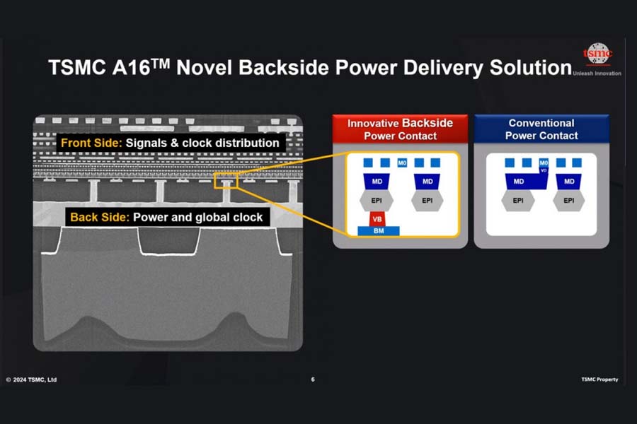 The A16 process integrates a backside power rail (Super Power Rail - SPR), enhancing power delivery and increasing transistor density. This combination of GAAFET transistors and BSPDN technology results in notable improvements:
 TSMC's adoption of BSPDN technology, specifically the Super Power Rail variant, distinguishes it from other fabs pursuing similar approaches. Furthermore, the industry is witnessing a shift in process node naming conventions, moving towards smaller denominations such as the "Angstrom era" to reflect the increasingly advanced technology.
TSMC 1.66nm Process node Overview
Advanced Transistor Technology and Power Delivery
Technical Advantages
- 8-10% performance boost at the same voltage and complexity.
- 15-20% reduction in power consumption at the same frequency and transistor count.
- Up to 10% more transistors can be accommodated, depending on chip design.
Targeted Applications
TSMC's A16 node is positioned to cater to high-performance computing products, particularly AI and HPC processors that require complex signal routing and dense power circuitry. The backside power delivery network is particularly advantageous for AI and HPC applications, enhancing performance and power efficiency.Industry Context
- Also, read
TSMC 1.66nm Process Node Production date
TSMC plans to start volume production of the A16 node in the second half of 2026. Consumer-ready products based on this advanced manufacturing process are expected to hit the market in 2027.- Meanwhile, watch our review of Oppo Reno 11F
Article Last updated: April 26, 2024