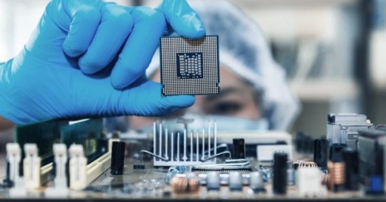
The term "nanometer" (nm) is commonly used when talking about chipsets. For example, the Snapdragon 8 Elite features a “3nm” process, while the MediaTek Dimensity 9000 uses a “4nm” process. Have you ever wondered what exactly is this technical term? Basically, nanometer is a unit of measurement that refers to the size of transistors in modern semiconductors. In this article, we'll dive into the depth of nanometers and clear up some common misconceptions regarding the matter.
Nanometer in Chipset
Well, I have already mentioned that a nanometer measures the size of transistors, but what is a transistor again?What are Transistors?
In simple words, transistors act as electronic switches. Generally, binary systems are used for storing data, where information is encoded as a series of ones “on” and zeros “off”. And in the past, vacuum tubes served as the first reliable electronic switches in this process. However, these tubes consumed a lot of power and were prone to breaking. So researchers developed "transistors" as a more refined version of those vacuum tubes.- Also, read:
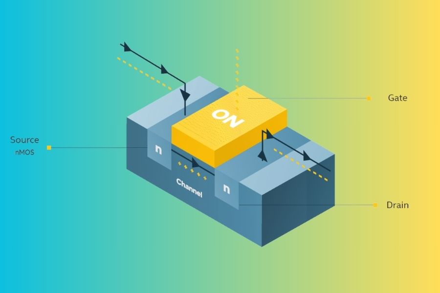
Structure of a Transistor
A transistor consists of three parts: the Drain, the Source, and the Gate. The current flows from the Source to the Drain through a channel controlled by the Gate. Here, a shorter Gate Length means that a transistor can quickly turn on and off and this length is typically what is indicated by 'nanometer'. This means that more data can be processed quicker and you get a faster computer. All that means for you and me is that typically a smaller nanometer size corresponds to a shorter length and faster channel resulting in improved performance.Nanometer today
What I’ve explained above is mostly accurate, especially if we look back a decade or two. But as technology has progressed, the relationship between the node name (like 7nm or 5nm) and the actual size of the transistor has become less direct. For instance, the "7nm" or "5nm" process doesn’t necessarily correspond to the gate length or specific dimensions anymore. Instead, these terms now reflect a generation of technology that brings improvements in transistor density, power efficiency, and performance, rather than a direct scaling down of the physical size.Marketing behind Nanometer Nodes
Companies like Intel, TSMC, and Samsung now use the nanometer node as more of a marketing tool. A smaller node number suggests a more advanced and capable manufacturing process, even if the actual dimensions don’t exactly match the node name. Some of this naming has shifted more toward marketing than technical accuracy. Let’s talk about one of the examples. Intel’s 10nm process was seen as comparable to TSMC’s 7nm process in terms of transistor density and performance. The company later rebranded its 10nm Enhanced SuperFin process as "Intel 7," and upcoming nodes are now called "Intel 4" and "Intel 3."Conclusion
So, while the term "nanometer" still carries weight, it’s more about signaling progress in technology than it is about precise measurements. Now, new processes generally mean denser and more efficient chips.- Meanwhile, watch our Snapdragon 8 Elite vs A18 Pro vs Dimensity 9400 video:
Article Last updated: January 31, 2025
![Hollyland LARK MAX 2 Price in Nepal [Updated 2026]](https://media.gadgetbytenepal.com/2025/08/Hollyland-LARK-MAX-2-price-in-Nepal-1.jpg)